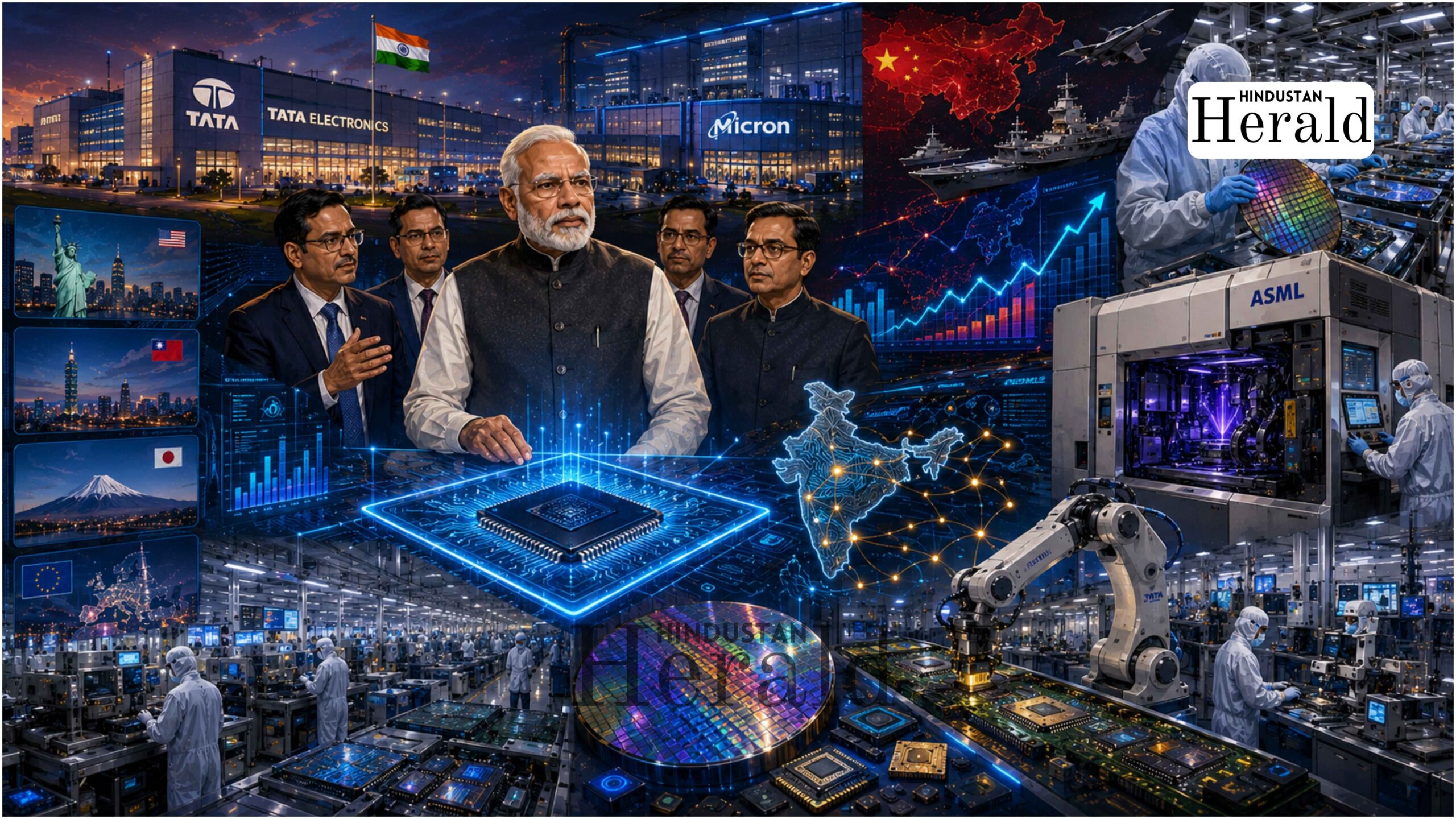
New Delhi, May 20: India’s semiconductor ambitions have never lacked for announcements. What they have lacked, historically, is staying power. That may be about to change.
The Union Ministry of Electronics and Information Technology (MeitY) is understood to be weighing an extension of the India Semiconductor Mission (ISM) 2.0 to a 12-year implementation window a timeline that, if confirmed, would fundamentally alter how global chipmakers assess India as an investment destination.
No official announcement has been made. The proposal has not yet cleared the Cabinet Committee on Economic Affairs (CCEA). But the fact that a 12-year horizon is even being discussed inside the ministry says something significant about how far India’s semiconductor conversation has travelled since the early days of bold press releases and limited follow-through.
How India Got Here
Cast your mind back to December 2021. The government had just launched the Semicon India Programme with a headline outlay of Rs 76,000 crore and considerable fanfare. Sceptics and there were many pointed to India’s long history of ambitious electronics manufacturing targets that quietly faded away. The country was importing chips worth over $24 billion a year and had no fab to speak of. The gap between ambition and reality was vast. What followed over the next three years was, by any honest reading, more progress than most industry watchers had expected.

In June 2023, Micron Technology announced a $2.75 billion assembly, testing, marking, and packaging plant in Sanand, Gujarat the announcement came during Prime Minister Narendra Modi’s state visit to Washington and carried the unmistakable weight of geopolitical choreography. But the project itself is real. Construction is underway. It will be India’s first foreign-invested semiconductor facility of genuine scale.
Shortly after, the government approved the Tata Electronics-Powerchip Semiconductor (PSMC) fabrication plant in Dholera, Gujarat valued at roughly Rs 91,000 crore, with the Centre covering half the cost. This is the one that actually matters most for India’s long-term chip ambitions. A fab that manufactures at the 28-nanometre node and above, targeting automotive electronics, defence systems, and consumer devices. The third approval, the CG Power-Renesas OSAT facility in Sanand, rounds out the picture with backend assembly and testing capabilities.
Three approvals in three years. For a country that spent most of the previous two decades watching Taiwan, South Korea, and China build chip empires while India talked about its engineering talent that is a meaningful start. Still, a start is all it is.
The Problem With Five-Year Thinking
Here is the uncomfortable truth about semiconductor investment that most policy discussions tend to skip over. By the time a fab goes from approved project to commercially viable facility, a typical five-year policy window is already expiring.
Civil construction alone on a greenfield fab takes two to three years. Getting the cleanrooms right, installing equipment from ASML, Applied Materials, and Lam Research, qualifying the tools, developing the process, improving yields, completing customer qualification that adds another three to four years at minimum. And that is if everything goes smoothly, which in semiconductor manufacturing, it rarely does.
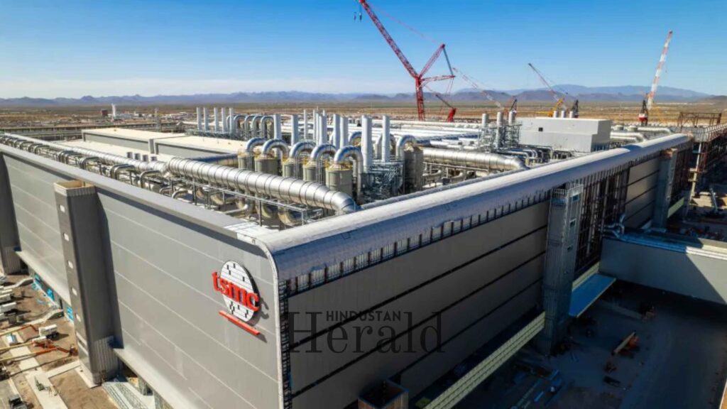
TSMC’s Arizona facility backed by one of the most experienced chip companies in the world, in a country with deep semiconductor infrastructure still ran into construction delays and workforce challenges. India, building its first serious fab, will face steeper learning curves.
What investors need, therefore, is not just a generous incentive today. They need confidence that the incentive framework will still be intact when the fab starts generating revenue which could be seven, eight, or nine years from the date of approval. A 12-year policy window addresses this directly. It tells a chipmaker or OSAT player: you will not be building into a policy vacuum. That assurance, more than the percentage of subsidy, is what moves investment committees.
What The Mission Still Needs To Fix
It would be misleading to paint ISM’s progress without acknowledging how much ground India still needs to cover. The chip design side of the equation looks relatively healthy. India hosts over 3,000 semiconductor design companies and captive design centres, including major units run by Qualcomm, Intel, Texas Instruments, NXP, and MediaTek. The country is estimated to produce roughly 20 percent of the world’s chip design engineers. Bengaluru, Hyderabad, and Pune are genuine global design hubs, not just aspirational ones. But the deeper you go into the manufacturing supply chain, the thinner India’s capabilities become.
Take photomasks the templates used to transfer circuit patterns onto silicon wafers. India has no meaningful domestic photomask industry. Every mask used in the Tata-PSMC fab will need to be sourced internationally, which creates both cost and supply chain vulnerability. Or consider ultra-pure process chemicals photoresists, etchants, CMP slurries the kind of highly specialised materials whose global supply is dominated by a handful of Japanese and German companies. India produces almost none of these at semiconductor grade.
Then there is the workforce gap that does not get discussed enough. India graduates enormous numbers of engineers every year. But running a fab requires a very specific kind of worker process engineers, equipment engineers, yield specialists, cleanroom-trained technicians. These people do not come out of standard engineering curricula. They need dedicated training, ideally on actual equipment, and that pipeline takes years to build.
According to reporting by The Economic Times, ISM 2.0 is likely to take a more deliberate approach to these gaps with stronger emphasis on compound semiconductors like gallium nitride and silicon carbide for EV and 5G applications, a dedicated workforce development programme, and policy support for domestic chip design IP.
Whether these components make it into the final framework in meaningful form, or get diluted into vague commitments, will determine much of ISM 2.0’s real-world impact.
Reading The Geopolitical Room
India is not building its semiconductor industry in a vacuum. The global chip landscape has fundamentally shifted since 2020, and much of that shift works in India’s favour but only if it moves fast enough to capitalise.
The US CHIPS and Science Act committed $52.7 billion to domestic semiconductor manufacturing and explicitly encouraged allied nations to build parallel capacities. India, as a Quad partner and increasingly close strategic ally of Washington, fits neatly into that framework. American chipmakers investing in India can position those investments as part of a broader allied-nation supply chain diversification which makes the political story easier on both sides.
The European Chips Act, Japan’s RAPIDUS initiative, and South Korea’s K-Chips Act are all working from the same playbook use state capital to anchor domestic chip capacity before the geopolitical window narrows further.
The risk, of course, is that everyone is playing the same game simultaneously. TSMC’s Kumamoto fab in Japan is already producing. Its Arizona plants are ramping. Samsung’s Taylor, Texas facility, despite delays, remains committed. Every dollar of semiconductor capex that goes to Japan, the US, or Europe is a dollar that does not come to India.
India has genuine advantages a large domestic electronics market, competitive land costs, significant engineering talent, and a government that is, for the first time in memory, treating semiconductor policy as a serious long-term priority. But advantages do not automatically translate into investment. They need to be backed by execution, and execution in this sector is brutally unforgiving.
What The Numbers Tell Investors
The existing Rs 76,000 crore Semicon India Programme has not been fully disbursed all three approved projects are still in construction or early phases, and the bulk of government payments will flow through 2025 and 2026 as milestones are reached.
ISM 2.0 is expected to come with a substantially larger war chest. Estimates cited by Business Standard and Mint suggest a potential outlay of Rs 1.5 to 2 lakh crore over the 12-year window though the ministry has not confirmed any figure. The government is also reportedly revisiting whether the existing split of 50 percent fiscal support for fabs and 30 percent for ATMP and OSAT facilities should be recalibrated for advanced-node investments or strategic sectors like defence semiconductors.
One change that the industry has been lobbying for consistently and which ISM 2.0 is expected to address is a more efficient single-window clearance process. Several companies that applied under ISM 1.0 and did not make the cut have pointed to land allocation delays, environmental clearance bottlenecks, and inter-ministerial friction as genuine deterrents. Fixing these is less glamorous than announcing a new incentive scheme, but arguably more important.
For market watchers, the ISM 2.0 development reinforces the investment thesis around a cluster of Indian companies directly exposed to the semiconductor buildout. Tata Electronics carries the most direct exposure through its Dholera commitment. Dixon Technologies and Kaynes Technology sit in the electronics manufacturing services space that feeds semiconductor demand. Avalon Technologies has a footprint in high-reliability electronics for defence and industrial markets.
Vedanta is worth watching separately. The company’s original semiconductor plan a joint venture with Foxconn that collapsed in 2023 left it without a technology partner. It has since signalled intent to find an alternative route into the sector. A new application window under ISM 2.0, particularly if eligibility criteria are revised, could give Vedanta a second shot.
The Longer View
There is a version of India’s semiconductor story that ends in the same place as many previous industrial policy attempts with promising starts, structural gaps that prove too wide to bridge, and eventual stagnation. That version is not impossible.
But there is another version. One where the 12-year ISM 2.0 commitment provides the policy stability that unlocks a second and third wave of investment. Where the Tata fab at Dholera proves the model for more advanced nodes. Where India’s chip design strength finally connects to domestic manufacturing in a meaningful way. Where the country that imports $100 billion worth of semiconductors annually by the end of this decade starts, gradually, to make some of them itself.
The 12-year horizon being discussed inside MeitY is not a guarantee of that outcome. But it is, at minimum, evidence that the people writing India’s chip policy understand what the industry actually requires. That alone is more than could have been said five years ago.
Stay ahead with Hindustan Herald — bringing you trusted news, sharp analysis, and stories that matter across Politics, Business, Technology, Sports, Entertainment, Lifestyle, and more.
Connect with us on Facebook, Instagram, X (Twitter), LinkedIn, YouTube, and join our Telegram community @hindustanherald for real-time updates.

Tracking world politics, global markets, trade movements, policy decisions, and the changing balance of economic power.
- Shelesh Joshi

- Shelesh Joshi
- Shelesh Joshi
- Shelesh Joshi


Former financial consultant turned journalist, reporting on markets, industry trends, and economic policy.
- Kavita Iyer
- Kavita Iyer
- Kavita Iyer
- Kavita Iyer